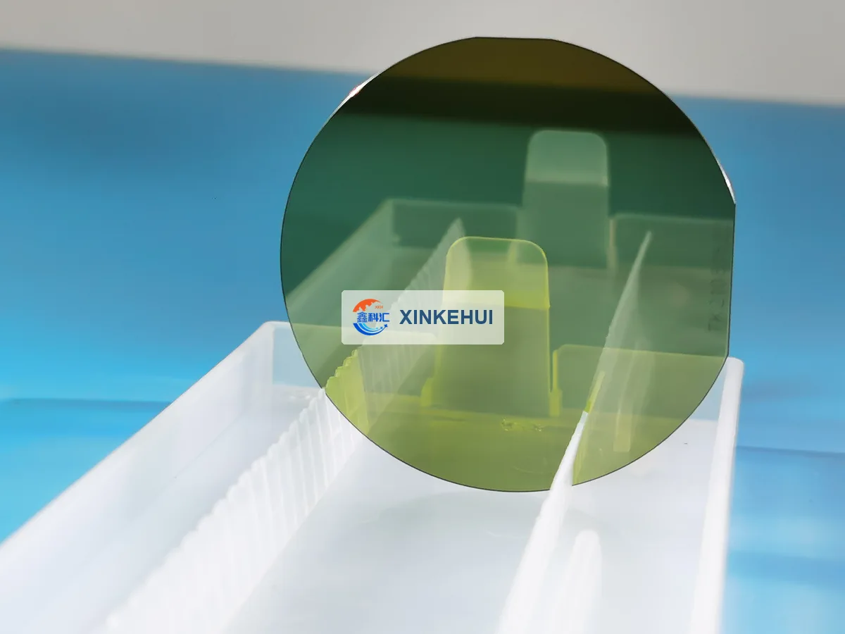
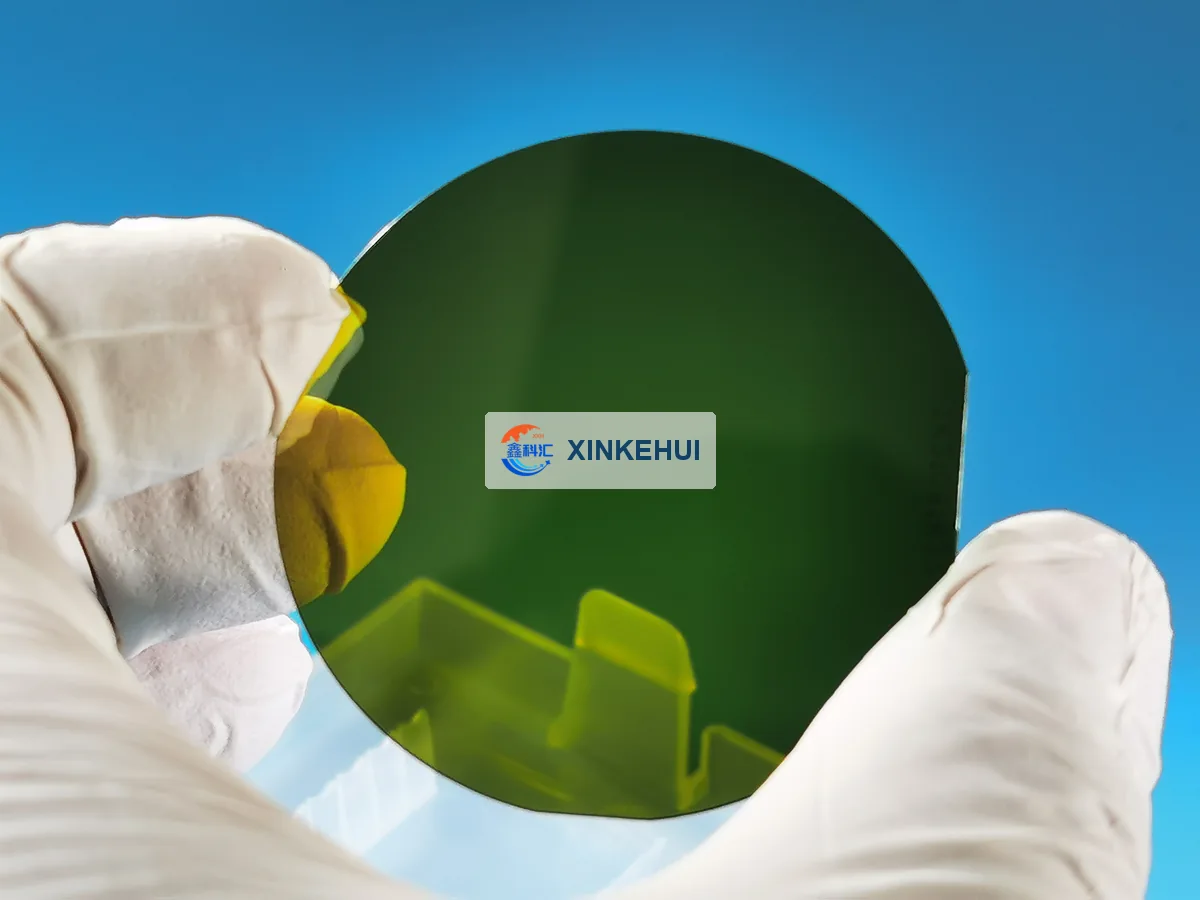
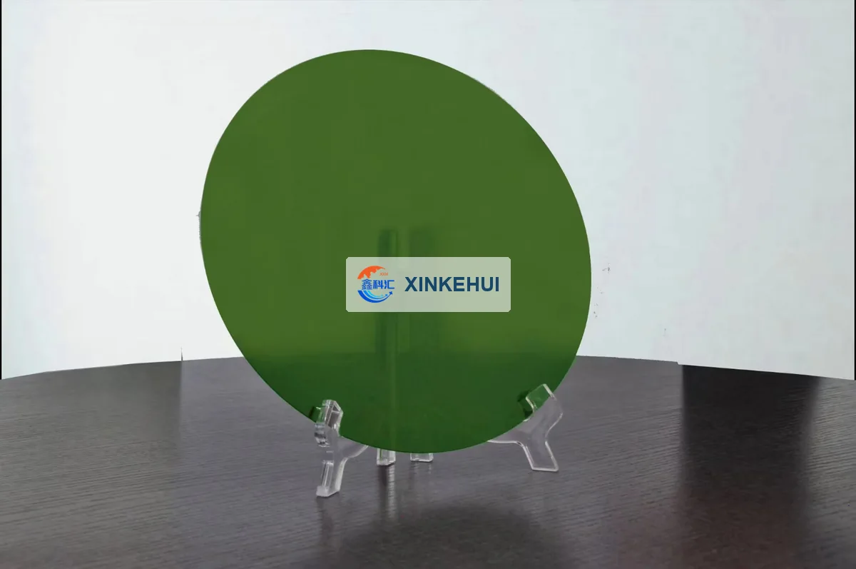
XINKEHUI silicon carbide wafer sample held with clean gloves

SINGLE CRYSTAL. NEW POSSIBILITIES.

Silicon Carbide
Wafers

The foundation for next-generation power.
4H-N SiC wafers, precision substrates and single crystals for the ideas that move industry forward.

2–8 inch wafers4H-N & HPSICMP / MP finish
01 / SiC material sampleActual product photography

ENGINEERED FOR
A higher-performing world.

Electric mobility
Clean energy
Industrial power
RF & research

01 / MATERIAL PORTFOLIO

The right SiC.
For the right process.

From conductive 4H-N SiC wafers to semi-insulating substrates and SiC single crystals, start with the material your device architecture actually needs.

Representative polished SiC wafer with green appearance under ambient lightingCORE MATERIAL

POWER DEVICE SUBSTRATES

4H-N SiC Wafers

Nitrogen-doped, conductive silicon carbide substrates for SiC epitaxy and subsequent MOSFET or Schottky diode development.

  • 2, 3, 4, 6 and 8 inch SiC wafer formats
  • Production, research, dummy & seed grades
  • Surface finish and orientation by specification
Compare SiC wafer parameters
Representative silicon carbide sample showing a polished surface on a supportAPPLICATION-SPECIFIC

RF & EPITAXIAL PLATFORMS

Semi-Insulating SiC

4H semi-insulating and high-purity semi-insulating SiC substrates for projects requiring electrical isolation rather than a conductive current path.

  • GaN-on-SiC RF development
  • High-resistivity substrate requirements
  • Diameter and acceptance limits by quotation
Discuss your SiC substrate
Backlit silicon carbide wafer sample; appearance varies with illuminationCRYSTAL GROWTH & R&D

SINGLE CRYSTAL MATERIALS

SiC Crystals & Seed Wafers

SiC single crystal ingots and seed wafers for crystal growth, materials characterization and substrate development projects.

  • 2–6 inch ingot range in company literature
  • Conductive and semi-insulating enquiries
  • Seed face, thickness and orientation to agree
Specify a crystal or seed

Photos show representative SiC wafer samples, not a certification of diameter, conductivity or grade. Single crystal ingots are not pictured. All products are quoted against a confirmed specification.

02 / APPLICATIONS

Small substrate.
Significant impact.

SiC wafers sit at the beginning of a device manufacturing chain. Choosing the right silicon carbide substrate helps align epitaxy, defect control and device design with the final application.

01

Electrifying the road ahead.

Conductive 4H-N SiC wafers support the epitaxial platform used to fabricate vertical SiC power devices. In electric vehicles, these devices are used in traction inverters, on-board chargers and DC–DC converters.

SiC switching devices can reduce conversion losses and support compact, high-power-density designs. A SiC substrate alone does not establish vehicle range, efficiency or automotive qualification.

Discuss power-device SiC wafers

Where SiC devices work

Traction inverters
Battery DC to motor AC conversion, with switching and conduction losses as key design considerations.
On-board & fast charging
High-frequency conversion stages where system efficiency, thermal design and packaging matter.
DC–DC conversion
Power transfer between voltage domains in an electrified vehicle.

SiC wafer selection: agree 4H-N conductivity, resistivity, off-axis direction, CMP surface, BPD/TSD limits and lot-specific inspection data.

Application context describes the use of finished semiconductor devices or epitaxial structures, not a claim that an unprocessed SiC wafer is a complete device. Technical references

03 / MATERIAL ADVANTAGES

A stronger starting point.

Understand what silicon carbide brings to a device platform, and what must still be verified at the SiC wafer and process level.

Wide-bandgap platform

4H-SiC provides a wide bandgap and high critical electric field, enabling power-device architectures beyond conventional silicon.

Thermal performance

SiC supports heat flow in high-power structures. Thermal performance varies with crystal quality, doping, temperature and device construction.

Surface preparation

CMP and MP options address different SiC wafer needs. For epitaxy, specify the target face, roughness and surface acceptance criteria.

Specification-led selection

Diameter is only the beginning. SiC substrate geometry, resistivity, orientation and defect limits must match your process.

4HHexagonal SiC polytype
N-typeConductive power-device route
HPSIHigh-purity semi-insulating option

Intrinsic material benefits do not imply guaranteed device yield, loss reduction or automotive compliance.

04 / TECHNICAL SPECIFICATIONS

Details make the difference.

Specification guide

SiC wafer portfolio

Company profile · page 21

Published portfolio values for SiC wafers. These are reference specifications, not confirmation of current stock or a universal acceptance certificate. Confirm your SiC wafer grade and lot requirements in the quotation.

SiC substrate dimensions and reference quality parameters
Parameter2 inch3 inch4 inch6 inch8 inch
Diameter50.8 ± 0.3 mm76.2 ± 0.3 mm100 ± 0.5 mm150 ± 0.5 mm200 mm nominal*
SiC types listed4H-N / HPSI / 4H-SEMI
6H-N / 6H-SEMI
4H-N / HPSI / 4H-SEMI4H-N / HPSI / 4H-SEMI4H-N / HPSI / 4H-SEMI4H-N / HPSI / 4H-SEMI*
Thickness options330 ± 25 µm
350 ± 25 µm
350 ± 25 µm
500 ± 25 µm
350 ± 25 µm
500 ± 25 µm
350 ± 25 µm
500 ± 25 µm
350 ± 25 µm
500 ± 25 µm
Surface roughness, Ra≤ 0.2 nm≤ 0.2 nm≤ 0.2 nm≤ 0.2 nm≤ 0.2 nm
Warp≤ 30 µm≤ 30 µm≤ 30 µm≤ 30 µm≤ 45 µm
Total thickness variation≤ 10 µm≤ 10 µm≤ 10 µm≤ 10 µm≤ 10 µm
Micropipe density< 1 cm−2< 1 cm−2< 1 cm−2< 1 cm−2< 1 cm−2
Polishing optionsCMP / MP; target face and inspection method to be confirmed
Edge options45° bevel / C-shape; edge geometry and applicable SEMI drawing to be agreed
SiC wafer gradesProduction grade for MOSFET / SBD; research; dummy; seed wafer

*The source prints the 8 inch tolerance as “± 03 mm”; it is not interpreted here. The profile lists 8 inch HPSI / semi-insulating types, while the public product overview specifically lists 2–6 inch semi-insulating SiC. Confirm 8 inch non-conductive formats with the team. Custom thickness is subject to review.

FOCUSED PRODUCT REFERENCE

150 mm
4H-N SiC substrate

The public 6 inch SiC product listing provides a more specific conductive substrate reference. These values belong to that listing and must not be substituted into every diameter or grade.

Request a 150 mm SiC quote
Diameter / thickness
150.0 ± 0.2 mm / 350 ± 25 µm
Conductivity / dopant
N-type / nitrogen
Resistivity
0.015–0.028 Ω·cm
Surface orientation
4° toward [11-20] ± 0.5°
Surface preparation
Double-side CMP; Si-face epi-ready
Published roughness
Si-face ≤ 0.2 nm; C-face ≤ 0.5 nm
Primary flat
47.5 ± 2.0 mm; // [11-20] ± 5°
Packaging options
Single-wafer or 25-wafer package
Defect / geometry limits
Grade-specific; written acceptance limits required

One order. One agreed specification. The public product listing and company profile use different geometry and quality limits. Your confirmed quotation, inspection method and lot documentation take precedence. Price range, current inventory and delivery time are not published; request confirmation.

05 / FROM ENQUIRY TO EVALUATION

Make your requirements clear.

A useful SiC wafer enquiry gives the material team enough detail to review suitability, supply options and inspection requirements before the order is placed.

  1. 01

    Define the application

    Power epitaxy, RF, crystal growth or process trials? State whether conductive or semi-insulating SiC is required.

  2. 02

    Set the specification

    Agree SiC wafer diameter, grade, thickness, face, off-cut, resistivity, finish and quantity.

  3. 03

    Review acceptance

    Request available SiC inspection data: geometry, roughness, crystal defects and measurement conditions.

  4. 04

    Confirm the order

    Approve the quotation, lot documentation, packaging, lead time and delivery terms before purchase.

What to include in your SiC wafer RFQ

Send your specification sheet or put the essentials in your enquiry.

  • Material, grade & wafer diameter
  • Thickness, orientation & polishing
  • Electrical & defect limits
  • Quantity, destination & timeline
An actual silicon carbide material sample from XINKEHUI company filesMaterials expertise.
Personal attention.

06 / ABOUT XINKEHUI

Material knowledge.
A practical partner.

Shanghai-based expertise in semiconductor substrates and optical crystal materials.

shanghai xinkehui new materails co.,ltd specializes in the development, production, processing and sales of semiconductor and crystal materials. Our portfolio includes SiC wafers, silicon wafers, sapphire substrates, CVD synthetic diamond, YAG single crystals, ZnSe windows and sapphire watch components.

The company introduction describes an experienced engineering team, precision processing and inspection capabilities, and support for non-standard requirements. This SiC material page brings the wafer and crystal portfolio into focus, so you can discuss a specific process with our team.

Semiconductor materialsSubstrates, wafers and single crystals
Requirement-led serviceTechnical review before quotation
Start a materials conversation

08 / FREQUENTLY ASKED QUESTIONS

Answers before
your next step.

Practical guidance for selecting and ordering SiC wafers and silicon carbide substrates.

Ask a specific question
What is a 4H-N SiC wafer?

A 4H-N SiC wafer is a nitrogen-doped, N-type single crystal silicon carbide substrate with the 4H hexagonal polytype. It provides a conductive base for appropriate SiC epitaxial structures and power-device manufacturing processes.

Which SiC wafer diameters are listed?

The company profile lists 2, 3, 4, 6 and 8 inch SiC wafers, corresponding to nominal diameters of 50.8, 76.2, 100, 150 and 200 mm. The public overview lists 4H-N SiC across 2–8 inches. Current availability must be confirmed.

What is the difference between N-type and semi-insulating SiC?

N-type SiC substrates are conductive and are commonly used for vertical power-device platforms. Semi-insulating SiC substrates have much higher resistivity and are used where electrical isolation is needed, including GaN-on-SiC RF structures. These materials are not interchangeable.

Are SiC wafers supplied with an epitaxial layer?

The main specification table describes SiC substrates, not a defined epitaxial stack. The public overview separately mentions 4–6 inch SiC epitaxial wafers. For epitaxy enquiries, specify layer thickness, doping, uniformity and defects so the team can review the requirement.

What resistivity is published for 150 mm 4H-N SiC?

The public 6 inch conductive SiC listing gives a resistivity of 0.015–0.028 Ω·cm with nitrogen doping. This value is not a universal specification for all SiC wafers and must not be applied to semi-insulating SiC substrates.

Why is a 4° off-axis orientation used?

An off-axis SiC surface is used in many epitaxial processes to support controlled step-flow growth. The public 150 mm 4H-N listing specifies 4° toward [11-20] ± 0.5°. Confirm the surface face, direction and tolerance against your epitaxy process.

What do CMP and MP mean for SiC wafers?

CMP means chemical mechanical polishing; MP means mechanical polishing. They describe different surface preparation routes. For an epi-ready SiC substrate, agree the target face, roughness, surface damage criteria and cleaning condition rather than relying on the polishing label alone.

How do production, research and dummy grades differ?

SiC wafer grades address different acceptance criteria and intended uses. Production-grade SiC requires process-specific electrical, geometric, surface and crystal-defect limits. Research grade is selected for the experiment; dummy grade is intended for tool or handling evaluation, not automatically device fabrication.

Which crystal defects should a SiC wafer enquiry cover?

Depending on your process, request limits and available measurements for micropipe density, basal plane dislocations, threading screw dislocations, polytype inclusions and surface defects. The portfolio MPD reference is below 1 cm−2, but grade-specific limits must be agreed in writing.

Can SiC wafer thickness or edge geometry be customized?

The company profile indicates customized thickness and lists bevel or C-shape edge options. Supply a drawing with SiC wafer diameter, thickness, tolerance, flat or notch, orientation and edge criteria. Manufacturing feasibility and pricing need technical review.

Are SiC single crystals and seed wafers offered?

The company literature lists 2–6 inch SiC ingots and wafers in conductive and semi-insulating types. Seed-wafer grade is also listed. Specify polytype, conductivity, face, orientation, diameter, thickness and crystal-defect requirements for confirmation.

What inspection documents should I request?

Request the available lot-specific inspection report and agree the required measurements before ordering SiC wafers. Possible items include dimensions, TTV, warp, roughness, orientation, resistivity and defect data. The document scope is subject to confirmation, not assumed for every grade.

What are the price range, stock status and delivery time?

No verified public price range or real-time stock record is supplied for these SiC wafers. Price and lead time depend on diameter, grade, quantity, surface finish and acceptance limits. Request a written quotation and inventory confirmation; this page does not promise immediate availability.

How should SiC wafers be stored and handled?

Keep SiC wafers in their specified protective packaging in a clean, dry environment. Use suitable clean gloves and wafer handling tools, avoid touching polished surfaces and follow your facility’s contamination-control procedure. Confirm the supplier’s packaging and cleaning instructions for the ordered lot.

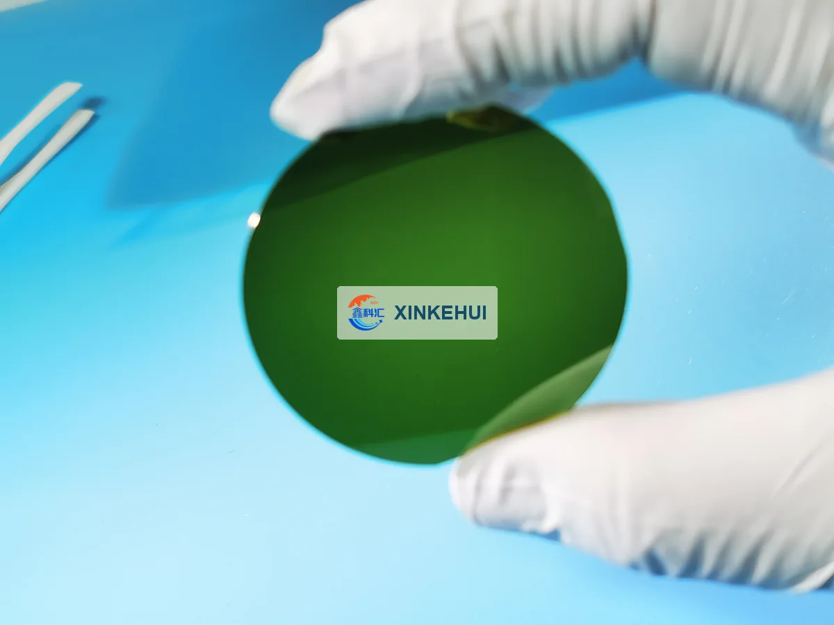
09 / LET'S TALK MATERIALS

Your next SiC project
starts here.

Share your specification. We will review the material, supply options and quotation requirements.

EMAIL[email protected]PHONE / WHATSAPP+86 132 6287 9223
SHANGHAI OFFICERoom 1805, Building 1, Wanda Mall,
1079 Dianshanhu Avenue, Qingpu District,
Shanghai, China
Connect on WhatsApp

Request a material quotation

An email or WhatsApp draft opens for your review. Your enquiry is sent only when you send it there.

Technical references

SiC specifications: XINKEHUI company profile (page 21), SiC crystal introduction (page 8), and the public product pages below. Application context is general technical guidance, not a product certification.

WhatsApp enquiry

Enquiry privacy

This page prepares your enquiry locally in your browser. It does not submit form data to a website server or save it in browser storage. When you open an email or WhatsApp draft, the details are handed to the service you select.

You send the draft yourself. XINKEHUI uses received enquiry details to review and respond to your material request. For privacy questions or a deletion request, contact [email protected]. Email and WhatsApp are subject to their respective providers' policies.